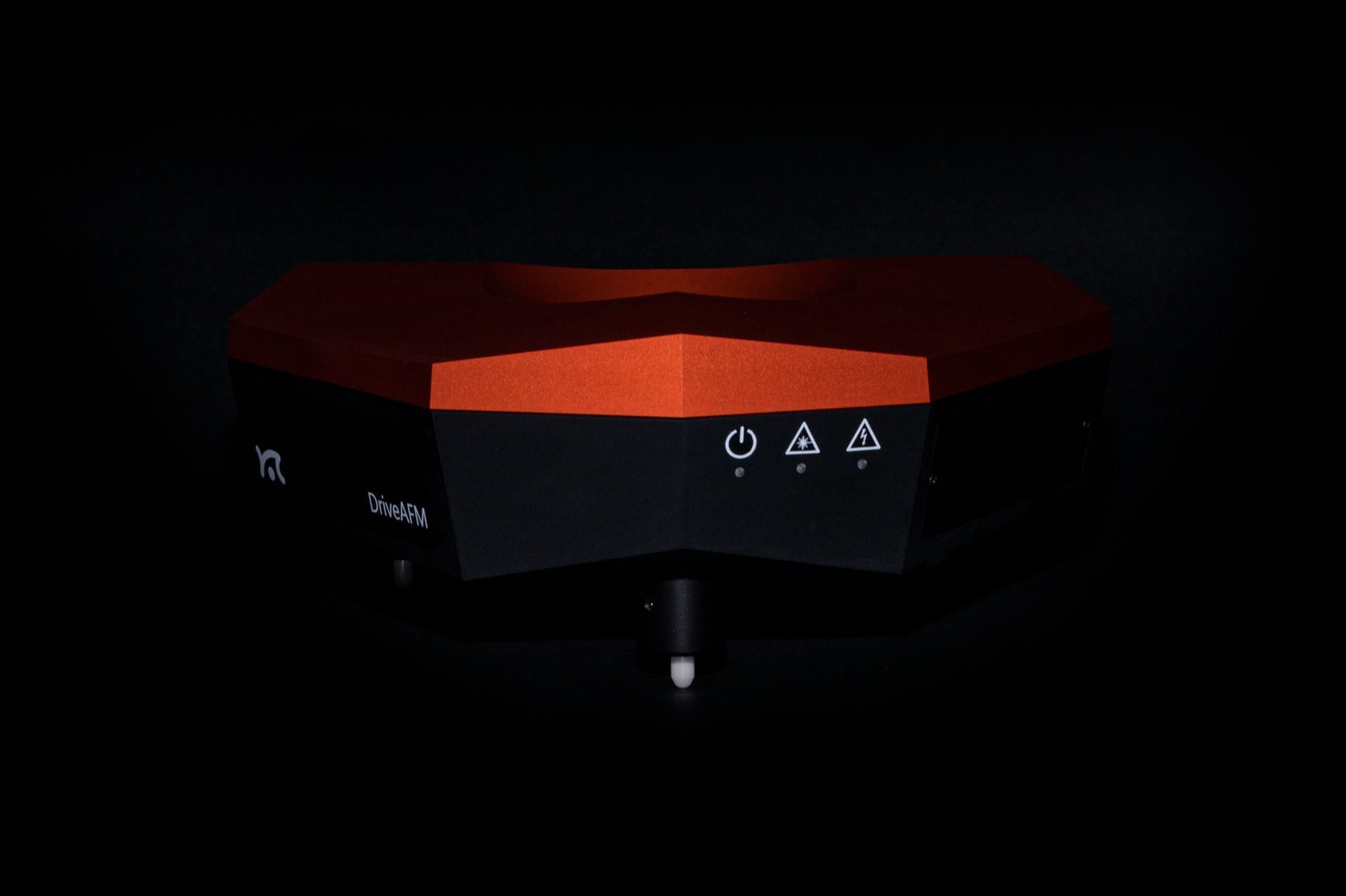
Nanosurf offers a variety of versatile research-grade atomic force microscopes for different types of users and requirements.
Life Science, Materials Research, Electronics
Nanosurf offers a variety of versatile research-grade atomic force microscopes for different types of users and requirements.
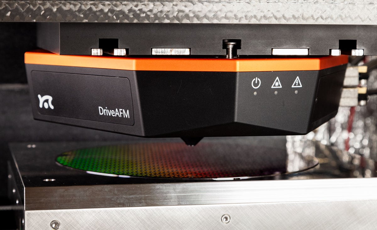
Wafers, Glass, and more
Nanosurf offers purpose-built solutions for various industrial applications and the option to build custom AFM systems.
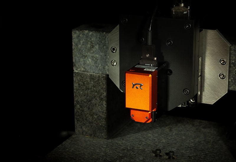
Special Requirements
AFMs suitable for integrating into existing setups or customized systems for special purposes.
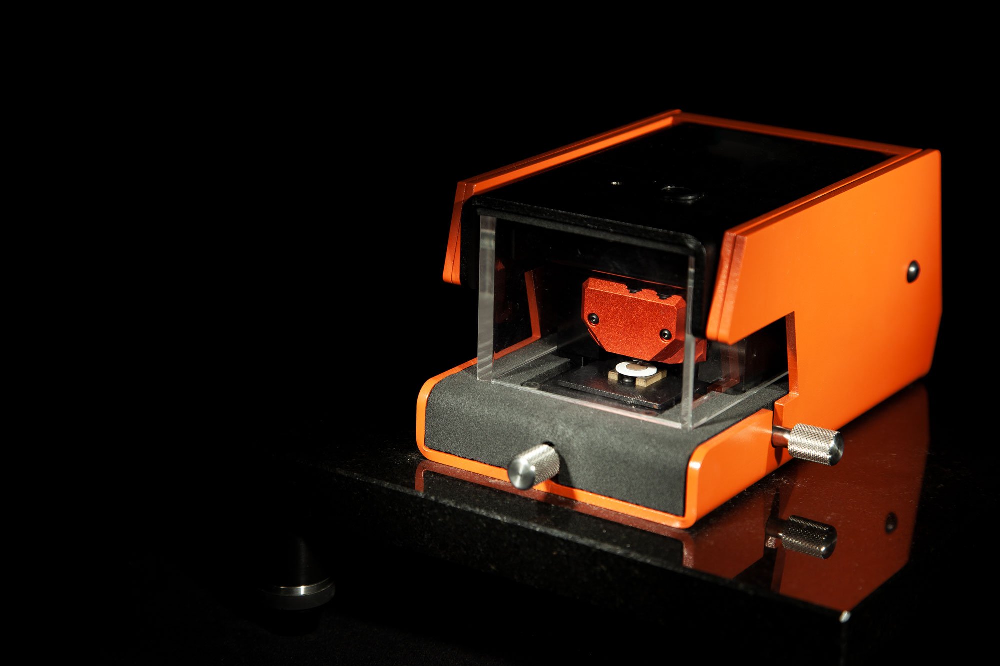
Education & Basic Research
Simple, robust, and easy to use instruments popular for educational settings and to perform basic research.
07 March 2025
Nanosurf welcomed University of Basel Nanoscience students for an in-depth tour of their facilities, showcas...
Read more
11 November 2024
How to measure mechanics of single cells
Read more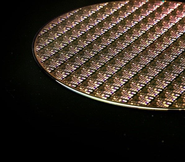
24 October 2024
Discover how Atomic Force Microscopy (AFM) is revolutionizing industries by providing unparalleled insights ...
Read more
10 September 2024
Explore the strengths and limitations of Atomic Force Microscopy (AFM), Scanning Electron Microscopy (SEM), ...
Read moreConference & Exhibit

13 May 2025 | 13 May 2025
EPFL, CH
CMi serves as a networking forum to present the past year's research achievements and encourage interaction among professors, researchers, students, and industry partners.
READ MOREConference & Exhibit

26 May 2025 | 30 May 2025
Madrid, ES
Multifrequency AFM Conference platform for experts and newcomers in force microscopy and nanomechanics to share knowledge on advanced atomic force microscopy instrumentation, methodologies, and theoretical aspects.
READ MOREConference & Exhibit
09 June 2025 | 13 June 2025
Trest, CZ
The purpose of the Discussions is to bring together, on invitation by the Organizing Committee, a limited group of specialists in a particular field of electrochemistry, and to enable them to exchange ideas and views on their research problems in an informal and friendly atmosphere.
READ MORE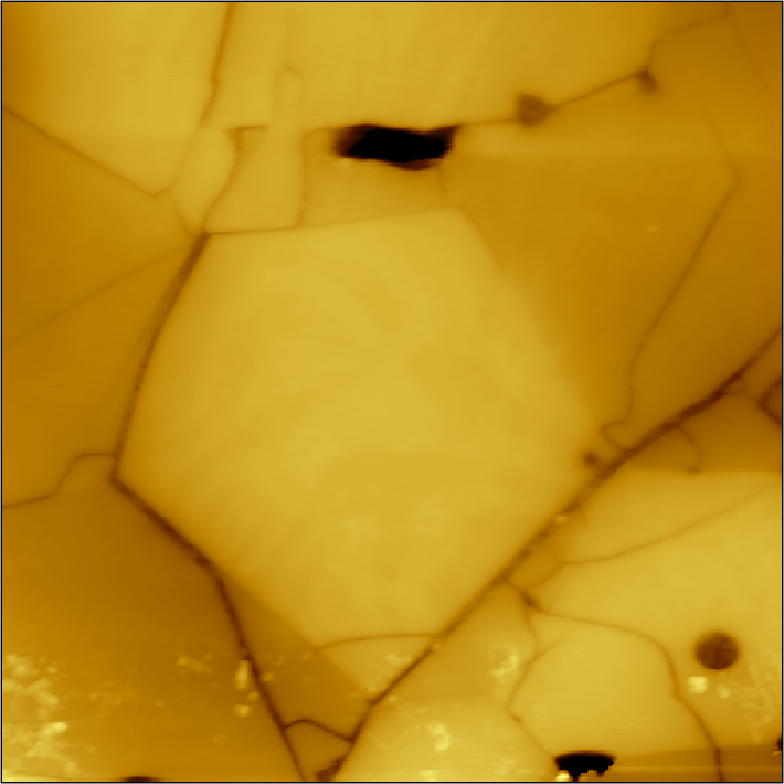
In-plane domains in ErMnO3 visualized using DFRT PFM
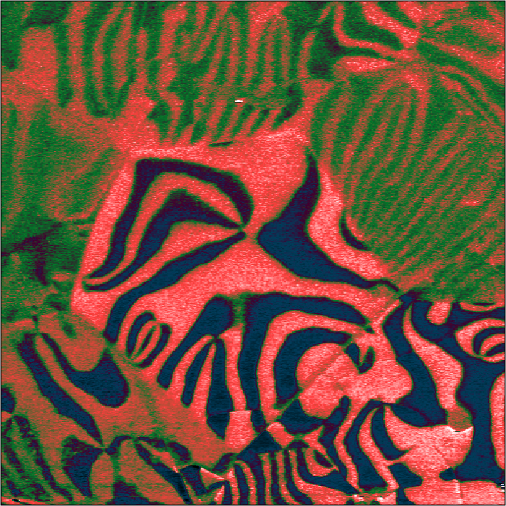
In-plane domains in ErMnO3 visualized using DFRT PFM
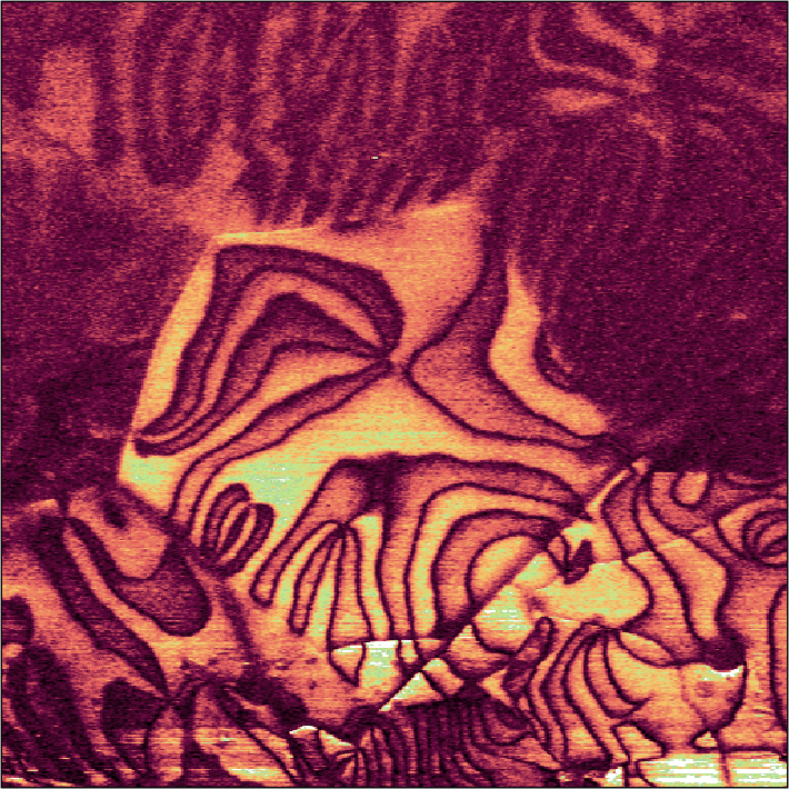
In-plane domains in ErMnO3 visualized using DFRT PFM
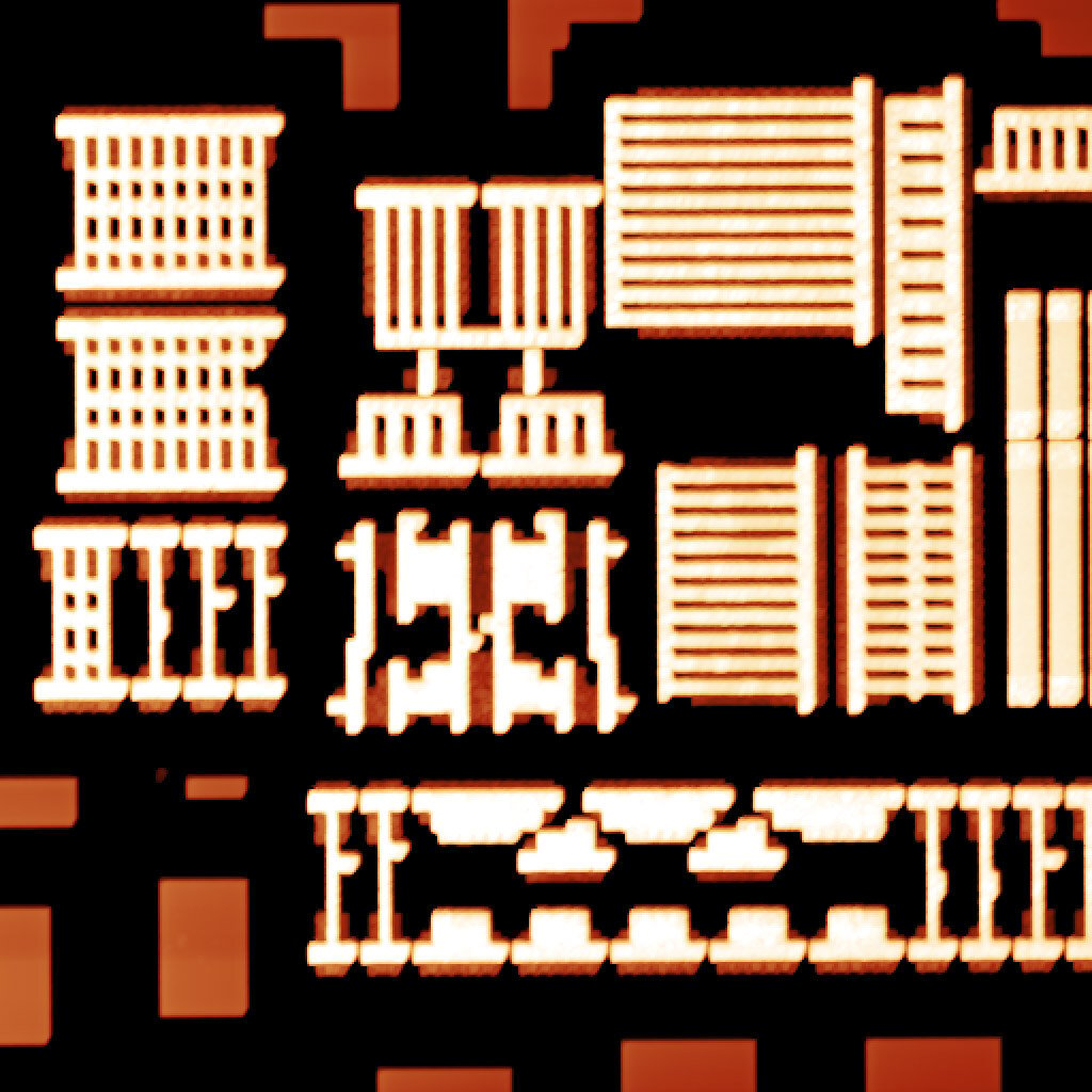
Topography of reverse-engineered silicon chip structure
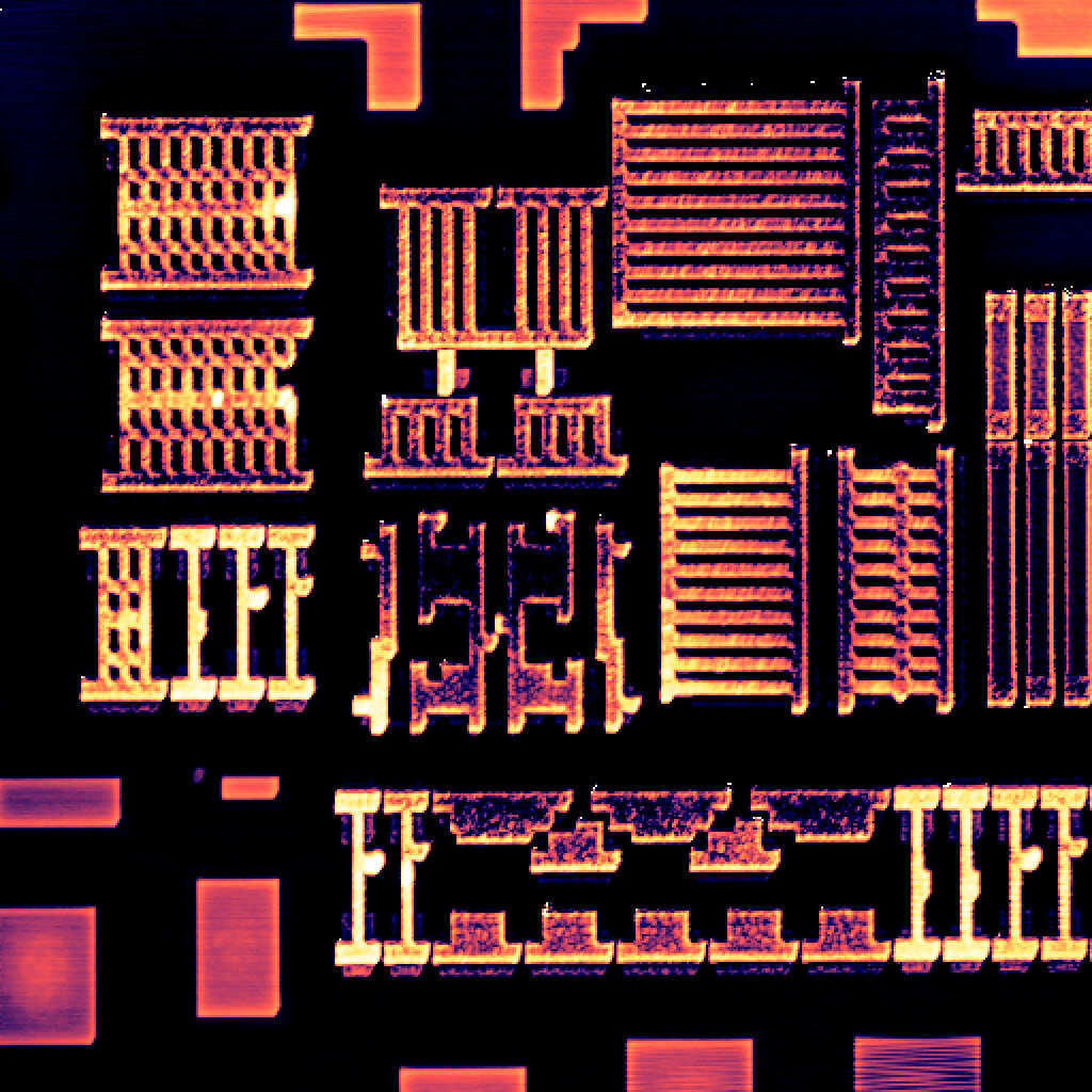
Real part of S11 parameter of reverse-engineered silicon chip structure
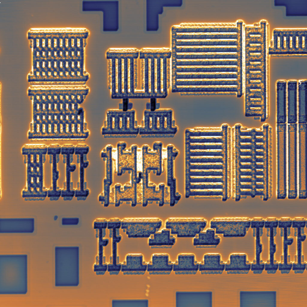
Imaginary part of S11 parameter of reverse-engineered silicon chip structure
Technical Note

This technical note gives a detailed overview of Nanosurf's WaveMode NMA technology for nanomechanical chara...
READ MOREApplication Note
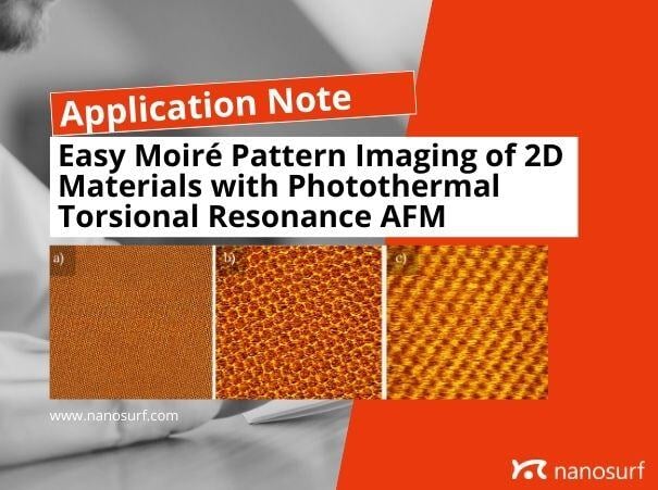
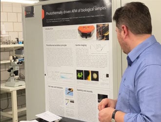
This application note discusses the application of photothermal torsional resonance in Atomic Force Microsco...
READ MORETechnical Note

This technical note discusses the advancements in viscoelastic characterization at the nanoscale using Atomi...
READ MOREApplication Note

This application note outlines the advancements in material characterization, specifically using Nanosurf’s ...
READ MOREApplication Note

Discover the advanced applications of electrical Atomic Force Microscopy in this white paper. Learn about el...
READ MOREApplication Note

In 2021 Nanosurf introduced CleanDrive - a clean and reliable way to oscillate an AFM cantilever using photo...
READ MORETechnical Note
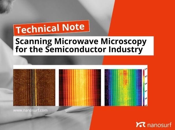
This application note explores the use of Scanning Microwave Microscopy in the semiconductor industry, highl...
READ MOREApplication Note

During last century humans have endured multiple severe viral outbreaks including the Spanish flu and other ...
READ MORE